Sunday, July 25, 2010

Erection During Male Genital Examination

Miniature Antenna Tower for Radio


Miniature Antenna Tower for Radio

Overview

The project uses a 4-element Yagi-Uda and some blinking lights at the top for transmission to create a miniature antenna tower project.

Explanation

The Yagi-Uda antenna is made of copper clad steel wire with 14 AWG for the vertical parts of the structure while the zigzag structure was made by wrapping around 18 AWG copper wire around s flat strip of steel. The coil is then stretched out so that it will resemble the zigzag structure of a real antenna tower . The 3 vertical pieces and 3 zigzag pieces were soldered together after being made followed by the thrust bearing plate and rotator plate that are made from small bits of PC board and some small coils of copper wire.
The circuit board used was made thin to fit between the box and the base tight. The flasher circuit was built around 555 and soldered to the box with a battery connector taken from a dead 9V battery. The active components include the triode, NPN BJT, bridge rectifier, P-channel MOSFET, diode, and pentode. The passive components comprise of iron core transformer, resistor, crystal, battery/DC power source, ground connection, antenna, electrolytic capacitor, inductor, and momentary/morse key switch.

ELABORADO POR:
NERWIN ANTONIO MORA REINOSO
C.I: 17.557.095
EES
SECCION 1

Worms That Help Make Yogurt

Speaker Box Audio Amp

Design Philosophy
I did this design after getting a new computer. After buying the processor, monitor, and printer, I wasn't willing to spring for a set of speakers too. After going "soundless", I decided to add speakers. Of course, this was the perfect excuse warm up the soldering iron to try out a new design. This original design is a variation on a well-known design, examples of which can be found in a great many texts. My variation was to add a second differential stage to replace the usual common emitter-plus-constant current source. Doing so opens up a second inverse feedback path. The signal path being a series connection of the differential amp inverting inputs, and the feedback being the non-inverting inputs. To this end, the constant current source does not include bypass capacitors to render it a DC-only stage. The other feedback path is the usual one: output to the non-inverting input of the first differential stage. The idea is to add lots of inverse feedback in order to linearize the output transistors, as the non-linearity of these devices makes them rather poor analog amplifiers.

The other design criterion was the use of components readily available at a hobbist's store: "Radio Shack". No "exotic" components that would require a special order are used here. To this end, the output stage is a semi-complementary design, although this is not optimum so far as fidelity is concerned. (Radio Shack doesn't offer complimentary pairs of power BJTs.) Since the amp is intended to work into the "wide band" (60Hz -- 18KHz) speakers that this store sells, the gain is deliberately kept down. With the design given here, the max output is 6.0W. Even here, since these speakers are rated at 3.0W, you could blow speakers if the volume is turned up too high. Limiting output is accomplished with the initial voltage amp (Q1). This stage has a gain of 7.5, so that with a 1.0VRMS input, the output voltage becomes slightly less than 7.5VRMS. The gain of the circuit from the output end of the volume control to the speaker is unity, due to the large negative feedback. You could drive the power output as high as 10W, as there is plenty of "head room" in the power supply design. (Again, this was done to improve the fidelity as much as possible with a BJT-based design.) If you push the output, you will need better heat sinking on the finals than what's described here.
The selection of actual components is not critical. Any small signal "transistors anonymous" will work here. The only exception is Q8 and Q10. These two must be a 2N3904 and a 2N3906, as these are complimentary pairs. These transistors set the characteristics for the entire final, and must be balanced as to characteristics in order to keep DC out of the speakers, and for symmetrical amplification. As for the differential pairs (Q2, Q3, Q5, Q6) type isn't so important, however, matched pairs is important. It's a good idea to get a couple dozen of each, PNP and NPN, and select pairs that match closely in VBE and hFE. Matching pairs in the differential stages helps hold down DC offset, as this design uses DC coupling in the interest of good low frequency response. Speakers tend to object to any significant amount of DC by burning out the voice coils. It also compromises fidelity in that DC on the voice coils restricts the movement of the cone.
The 1800pF capacitor connected to the drain of Q1 was included since one of these amps showed a weak (10mVP-P) oscillation at 700KHz. If you include it, be certain to make the connection with the least possible lead length, as it is an RF component. It will have no effect on the audio quality since its cutoff frequency is about 58KHz.
Construction: Amplifier
The entire unit is designed to fit in a plastic "project box" cabinet of 7 X 6 X 3 inches. The "wide band" speakers are 3¾ inches in diameter, and fit in a cutout of 37/16 inches. The circuit board is: 6¾ X 2¼ double-sided, copper clad. The circuit is built "dead bug" style, simply by making all ground connections by soldering to the unetched copper, the rest of the wiring being made above the circuit board. If additional mechanical reinforcement is needed, this is provided by soldering 2.2MEG resistors to the copper ground plane for use as a "tie point". Connecting such large resistors between the circuit and ground doesn't affect the operation since the impedance at that point is going to be several orders in magnitude smaller. To fit the circuit on the board, both sides are used. The preamp module being constructed on one side, with the final being built on the opposite side.
The heat sink for the power transistors is made from two pieces of steel or aluminum 1 X 1 (in.) angle stock. Simply measure off a 2¼ length, and cut it in half. This will naturally provide the necesary gap to separate these heat sinks electrically. Sand off enough copper from one end of the circuit board to insure that the heat sinks aren't being shorted out. These are attached to the circuit board with one screw and nut. (Also, be sure to clear the copper away from the screw heads on the preamp side of the circuit board, otherwise, you will short out the finals.) In the middle of one flange of the angle stock, bore a hole slightly smaller than the diameter of the 2N3053s. This hole should be enlarged by careful reaming, so that the transistors fit snugly. This is essential for good heat transfer out of the transistor and into the heat sink. Once this has been done, give the transistor a thin coat of silicone heat sink grease and press into place. These can be set aside until you need them.
Once the circuit is completed, and you've checked for wiring errors, the initial test is done with a 10 ohm/10W resistor connected to the output in place of the speaker. It is essential that this circuit, at no time, ever be run with no load. The Q3 DC return is solely through the load. If there is no load, this differential stage becomes severely unbalanced, and that will propagate to the finals, and probably blow one or both finals. The first thing to check is the DC voltage across the 10 ohm dummy load. This should be less than 0.5VDC. If there is more DC than that, then check each differential stage to see where that DC offset is coming from. This is most likely due to mismatched transistors (you did select for balance didn't you?) or finals too far out of match. When I did this construction, I didn't bother matching 2N3053s as the characteristics of the finals are determined largely by their Darlington counter parts. I didn't have any trouble from these components, but you can't rule the possibility out either. If the DC balance is acceptable, then you can either test with the dummy load, a signal generator, and an oscilloscope. You should see a faithful reproduction of the input wave form. If all goes well, then you can connect the speaker. When making this connection, it's a very good idea to connect the speaker return to the same point where the connection to the DC ground is made. This prevents the possibility of setting up an audio frequency ground loop. This, in turn, can cause instability that's next to impossible to fix. That means do not try to "one wire" the speaker if you decided to build the amp in a metal project box. Adjust the bias for 10 -- 15mA of no-signal idling current. You should then be good to go.
Construction: Power Supply
The power supply is simply a straight forward symmetrical plus/minus supply constructed from a transformer with a balanced secondary and a bridge rectifier module. Even though the transformer was a self-wound unit, any transformer with a 25.2VCT secondary at 2.0A will be a good substitute. Such transformers oughht to be available as VT "heater transformers" for high power "ham" RF amplifiers. It is essential that the primary side of the transformer be connected exactly as shown. This PS uses a MOV for over voltage protection. These things have a nasty habit of not turning off once they turn on. The fuse needs to be connected between this MOV and the mains. Don't attempt to "go cheap (or lazy)" and fail to include it. A 2.0A, "slow blow" type works well here. It will stand up to the initial surge as the filter capacitors charge up, and will prevent damage or worse should the MOV be triggered. This supply is somewhat over rated for the application, and is heavily bled for good voltage regulation. There is still some 120Hz hum that could be eliminated with a more involved PS circuit. However, as this wasn't intended as a "premium" amp, that wasn't necessary. The hum is most noticeable when running with no input signal. While actually playing sound, it's no longer noticeable. If you want to substitute a better supply, then that's OK, too.

Improvements
These units worked quite well, and do sound good, despite the inherent limitations of BJTs as analog amplifiers. There are a couple of improvements possible. The first would be the use of a full-complimentary final. If this is done, then any complimentary BJTs with a PC of 5.0W or more will work. Again, the most important part of this will remain the input Darlingtons. Even better would be the substitution of complimentary (N-Channel/P-Channel) VMOSFET power transistors. These, of course, don't require Darlington pairs in order to operate. If VMOS power transistors are used, it's important to include a 100 ohm resistor in series with the gate terminal, mounted close to the transistor body with the shortest lead length. This will help prevent the possibility of RF oscillation. (Unlike the BJT, the VFET is a high frequency device, and the inadvertant construction of VHF oscillators with these is quite easy.)
Parts List: Amplifier
CR1 -- 6: 1N914
Q1: 2N3819
NPN: 2N3904 (or other small signal NPN)
PNP: 2N3906 (or other small signal PNP)
Q8: 2N3904 (Critical)
Q10: 2N3906 (Critical)
Q9, 11: 2N3053
R<>: 1.0K/¼W miniature pot.
Parts List: Power Supply
C1 -- 2: 20000uF/35WVDC
CR1 -- 4: 50VPRV/5.0A Bridge Module
CR5: Green LED Panel Mount
F1: 2.0A, Slow Blow Fuse
T1: PRI: 120VRMS
SEC: 25.2VCT/2.0A
Z1: 120VRMS MOV

ELABORADO POR:
NERWIN ANTONIO MORA REINOSO
C.I: 17.557.095
EES
SECTION 1

Samsung Scx-4521f Copier Toner Empty

El transistor sin polarizar


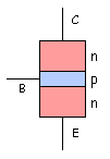
The transistor is composed of three areas of doping, as shown in the figure:


The upper zone is the "collector", the central area is the "Base" and the bottom is the "issuer". The Issuer is highly doped, the base has a very low doping, while the collector has an intermediate doping.
In this particular example the transistor is an npn device, but could be a pnp.
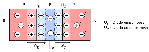
is similar in principle to two diodes A transistor looks like two diodes, the transistor has two connections: one between the emitter and the base and the other between the base and collector. The emitter and base are one of the diodes, while the collector and base form the other. These diodes are called "emitter diode (on the left in this case) and" collector diode (on the right in this case).


Before and after the broadcast

Let's do a study of the npn transistor, first when unpolarized (without batteries and open circuit) is a "diffusion" (as a gas in a bottle), where the electrons cross the area na p zone, diffuse, found a hole and recombine. This makes the joints between the n and p zones are created positive and negative ions.


This diffusion and recombination takes to reach equilibrium until a potential barrier of 0.7 V (for Si). 2 ZCE are created, one at the EB junction (W E) and in the CB junction.


PREPARED BY:
NERWIN ANTONIO MORA REINOSO
CI: 17,557,095
ESS SECTION 1

Getting High Lidocaine

TRANSISTORES DE POTENCIA


TRANSISTORES DE POTENCIA
the masconocidos

BJT TRANSISTORS

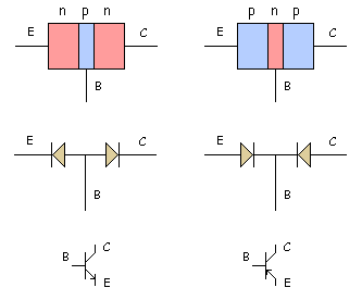
The transistor is the common bipolar transistors, and as transistors, can be germanium or silicon.


two types of transistors: the NPN and PNP, and the direction of current flow in each case is indicated by the arrow shown in the graph of each type of transistor


PREPARED BY:
NERWIN ANTONIO MORA REINOSO
CI: 17,557,095
ESS SECTION 1

Upper Back Pain In Pregnancy

CIRCUIT SPLINTERS


ok, here it is, as promised, AA's Circuit Splinter No.2! but first, a little warning- i am not an electrical engineer, nor do i claim to resemble anything close to one, here or on television. please take everything i post as just what it is- the off kilter ramblings of a misinformed diy enthusiast- nothing more, nothing less. i'm trying to learn just like you.

now-

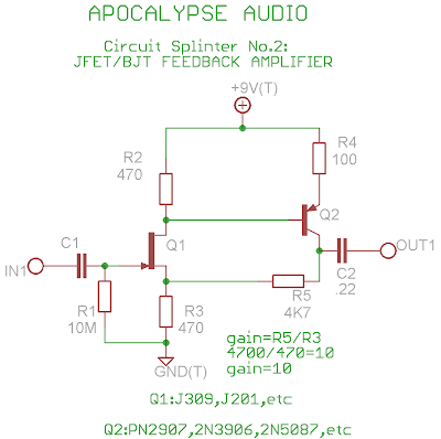
we are continuing our limited look into DC coupled buffers and amplifiers. in this case, a JFET/BJT Feedback Amplifier. this amplifier configuration is known as what is called a Sziklai Pair, otherwise known as a compound transistor, which is similar to a darlington pair, and sometimes called a compound darlington. this wikipedia article goes into the sziklai pair a bit more, such as how they are often used in discrete solid state output stages.


here is a great article as well from answers.com-

and finally, a jensen transformers app-note for a piezo buffer amp-


basically, what we have done that is different here from the last edition of Circuit Splinters(in my limited understanding), is to reduce the amount of feedback from one stage to the next. previously we had an infinite amount of feedback, which gave us a voltage gain of 0. by inserting R5 into the picture, we raise the resistance, and therefore lower the amount of feedback. in doing this, the gain of the stage rises. as you can see below, the gain of this stage is equal to the ratio of R3 to R5. so, lower R3, or raise R5, and the gain goes up. the circuit below has R3-470, R5-4700, so 4700/470 = a gain of 10. the great thing about this kind of stage is that you have a high input impedance from the FET, a buffered output, and you get voltage gain instead of just current gain as in a classic buffer. remember that R2 may have to be adjusted to 1/2 your supply voltage on the drain of Q1 for the proper amount of headroom.


i think that this circuit tends to sound best when used in a "clean" gain type of stage, with just a slight amount of breakup. never the less, many different adjustments can be made. instead of R3, put a large bypass cap, and move R3 to the emitter of Q2 for more gain. try different bypass caps for different frequency responses. bypass Q2's emitter. if you adjust your bias circuit, you can use a bjt for Q1. try a Ge pnp for Q2. see what happens when you put a small cap from the source of Q1 to the collector of Q2.

here is an example of an RIAA circuit that uses this configuration. you can see what has been done to tailor the frequency response of the stage for the RIAA curve using RC filters in the feedback section.
(click to enlarge)


here's a version from John Linsley Hood that uses a bootstrapped input-
(click to enlarge)


here's another one that uses a bjt for Q1, and has an interesting baxandall-style tone control based on feedback as well. note the bias configuration for the BJT input transistor.
(click to enlarge)


as always, if anyone out there has any real knowledge they can share, feel free! the sky's the limit. go nuts. have fun. take it easy!


ELABORADO POR:
NERWIN ANTONIO MORA REINOSO
C.I: 17.557.095
EES
SECCION 1

How To Fix Snowboard Epoxy

Frequency Response for MOSFET/BJT


The frequency response of a BJT or MOSFET can be found using nearly the exact same process, with the only variations being caused by a single resistor and simple naming conventions that differ between the two devices.
Before we start let's think a little bit about what we're doing:
Our goal is going to be to find the pole(s) of the circuit .
Okay? What is a pole and why do I care where it is?
A pole is a frequency at which the gain of the device rolls off. (remember that when it rolls off , it will be at the -3dB frequency with a slope of -20dB/decade)
We care because if the gain of a device rolls off at a certain frequency, then we won't be able to amplify a signal above that frequency very well because the gain will be decreasing by 20dB/decade.
The procedure is nearly identical whether we are using a BJT of a MOSFET, but we will work each of them side by side just in case there might be any confusion, and we'll follow these steps as we go through. (we will also use some values that came from the output file when running a simulation of this circuit in Cadence (or PSPICE) ) MOSFET
BJT
1. Take a look at one of the circuits and see what you notice, how about the MOSFET. This step is just to help us with our knowledge understanding of the circuit.
- At a glance it just looks just like another MOSFET right? Sure is, but let's take a look at a few things just for kicks. Notice that it is using a bypass capacitor at the source so we don't have to worry about R_s (at when working with high frequency). Since the capacitor C_s bypasses R_s to ground, you should notice that this is a common-source amplifier. You could notice the Values for R_1 and R_2 and start to think about what the Gate voltage is and how that may affect the circuit.
2. We are talking about frequency response so that means we are probably going to want to draw the small signal equivalent circuit.
Remember that the capacitors C_1 and C_2 will act like short circuits at high frequencies so we will ignore them, but we will have to account for some of the capacitance internal to the device.
Both devices have internal capacitances that are very similar. As you can see from the small signal models for a MOSFET (above) and BJT (below), the only significant difference is that the BJT has an additional resistance Rpi between the Base and Emitter.
Most of the analysis we will do is based on the small signal model. Note that small signal models are not typically used in PSPICE so this picture may look a bit odd, especially the controlled source but for our purpose it is good to have a visual reference. To start we will point out what everything is. Cgs is an internal capacitance betwe
en the gate and source. The
values for Cgs was similar to one the a PSPICE simulation may give. CM1 and CM2 are Miller capacitances which we will find values for later . ro is a Norton equivalent resistance that makes the model more ideal. And just pretend that the G2 looks more like a voltage controlled current source and that their gains are gm*Vgs and gm*Vpi. For the BJT CM1 and CM2 are both Miller capacitances, Cpi is similar to Cgs and Rpi the additional component used for BJTs but not MOSFETs. The other part should look familiar from the other figures.
ON TO THE ANALYSIS!!!
We will find the device gain, overall gain, equivalent input and output capacitances, and the input and output poles. The process for both is essentially the same.
Device Gain: This is the gain from the control source to the output so we are looking for Vout/Vgs (or Vout/Vpi for a BJT). We will ignore CM2 for this process. Notice the resistances ro, RD, and RL are in parallel. Vout should be given by that equivalent resistance times the current though it which is gm*Vgs from the control source. So the equation for device gain is,
V_{out} / V_{gs} = gm*(r_o//R_D//R_L) (MOSFET)
V_{out} / V_{\pi} = gm*(r_o//R_C//R_L) (BJT)
Overall Gain: This will be the gain from the source (Vs) to the output (Vout). We already know what Vout/Vgs is so if we find Vgs/Vs, we can multiply them to get Vout/Vs = (Vout/Vgs) * (Vgs/Vs). Vgs/Vs is a simple voltage divider. Hopefully you can see this from the small signal model (remember that we are ignoring the capacitors for now but they will play a part later). The equations we will get for Vgs/Vs and the overall gain are.
V_{gs} / V_s = \frac{ (R_1//R_2)}{(R_1//R_2) + R_s} (MOSFET)
Overall Gain: V_{out} / V_s = \frac{ (R_1//R_2)}{(R_1//R_2) + R_s} * gm(r_o//R_D//R_L) (MOSFET)
V_{gs} / V_s = \frac{ (R_1//R_2//r_\pi)}{(R_1//R_2//r_\pi) + R_s} (BJT)
Overall Gain: V_{out} / V_s = \frac{ (R_1//R_2//r_\pi)}{(R_1//R_2//r_\pi) + R_s} * gm(r_o//R_C//R_L) (BJT)
Now we will find the input and output poles. For this we will need to look at the capacitances and use a formula to find the Miller capacitances, CM1 and CM2. Any explanation for the miller capacitance will have to wait for another post or check out your Electronics Book , Wikipedia , Google , etc. but we will need to use a couple of special equations. Overall we will need to find the input resistance and input capacitance for the input pole and the output resistance and output capacitance for the output pole.
Each pole will be at a frequency w=1/RC where the R and C are the equivalent R and C at that point, so to find the input pole, we will need to find the input resistance and the input capacitance. These are found by looking into the input (the left side of the small signal model). The voltage source will act like a short so we see Rs in parallel with R1//R2 for the MOSFET (the BJT will have Rpi in parallel also). The input capacitance will be Cgs in parallel with CM1 (the BJT will be the same). The output resistance and capacitance are found the same way only looking in from the output (the right side of the small signal model).
\omega_{IN} = \frac{1}{R_{IN}C_{IN}} \omega_{OUT} = \frac{1}{R_{OUT}C_{OUT}} (MOSFET or BJT)
So the input pole will be: (MOSFET)
R_{IN} = R_S//R_1//R_2 = 950 R_{OUT} = r_o//R_D//R_L =
C_{IN} = C_{gs} + C_{M1} = C_{OUT} = C_{M2} =
\omega_{IN} = \omega_{OUT} =
(BJT)
and the output pole will be: (MOSFET)
(BJT)
R_{IN} = R_S//R_1//R_2//r_\pi = R_{OUT} = r_o//R_D//R_L =
C_{IN} = C_{BE} + C_{M1} = C_{OUT} = C_{M2} =

PREPARED BY:
NERWIN ANTONIO MORA REINOSO
CI: 17,557,095
ESS SECTION 1

Best Unrated Movie List

Diseño de un amplificador con BJT:


  • a gain of 10 a gain of 10
  • 50 K Ω or higher input impedance 50 K Ω or higher input impedance
  • 50 Ω or lower output impedance 50 Ω or lower output impedance
  • Low freq response: 20 Hz Low Frequency response: 20 Hz
  • High freq response: 100kHz. High Frequency Response: 100kHz.

Required: Required:

Design an amplifier using BJTs Design a BJT amplifier
The amplifier must-have: The amplifier must have:
  • a gain of 10 a gain of 10
  • 50 K Ω or higher input impedance 50 K Ω or higher input impedance
  • 50 Ω or lower output impedance 50 Ω or less output impedance
  • Low freq response: 20 Hz Low Frequency response: 20 Hz
  • High freq response: 100kHz High Frequency Response: 100kHz

1) Use Standard Resistor Values \u200b\u200b 1) Use standard values

resistance
We are going to use two stages for the amplifier , A common emitter stage Followed by a common collector stage. We will use two-stage amplifier, a common-emitter stage followed by a common collector stage.
Assuming β = 300, Vbe = 0.7 V, Vcc = 15 V Assuming that β = 300, VBE = 0.7 V, Vcc = 15 V

Common Collector Stage common collector stage

Let Rc2 = 2.2K Ω, Re2 = 2.2K Ω, VCEQ = 7.5 V That Tc2 = 2.2 K Ω, K = 2.2 Ω RE2, = 7.5 V VCEQ
Let
R3 / / R4 = Rth = 60 Ω That R3 / / R4 = 60 Ω Rth =
Solving for R3 & R4 Solving for R3 and R4
R3 = 188K Ω, R4 = 88K = 188K Ω Ω R3, R4 = 88K Ω

Using standard resistor values \u200b\u200busing the standard values \u200b\u200bof resistance

R3 = 220K Ω, R4 = R3 = 100K 220K Ω Ω, R4 = 100K Ω
Rth (new) = 68.75K Ω Rth (new) = 68.75K Ω

The Equivalent Circuit Ac ac equivalent circuit

Rout: omitting the output resistance of the first stage Path: The omission of the output resistance of the first stage
Which is Less Than 50 Ω What is less than 50 Ω

2) Common Emitter Stage 2) common-emitter stage

This stage must-have to gain = 10, and input impedance 50KΩ ≥ This stage should have a gain = 10, and ≥ 50KΩ input impedance
A rough Approximation for the gain ≈ Rc1/Re1 An approach to gain ≈ Rc1/Re1
Let Rc1 = 10k, RE1 = 820Ω, V = 7.5 VCEQ That Rc1 = 10k, Re1 = 820Ω, V = 7.5 VCEQ

The Equivalent Circuit Ac ac equivalent circuit

We want Rin Rin ≥ ≥ 50KΩ 50KΩ We
Rin = Rth / / Rib Rin = Rth / / Rib
50K = Rth / / 258K 50K = Rth / / 258k

Solving for Solving Rth Rth

Rth = Rth = 62KΩ 62KΩ
Solving R3 & R4 for Solving for R3 and R4
R1 = 658K Ω, R2 = 68K Ω Ω R1 = 658K, R2 = 68 K Ω

Using standard resistor values \u200b\u200busing the standard values \u200b\u200bof resistance

R1 = 470K + 220K Ω Ω Ω = 690K, R2 = 68K Ω R1 = 470K + 220K = 690K Ω Ω Ω, R2 = 68 K Ω
Rout = 10k Ω Rc1 = Path = = 10K Ω Rc1

3) Frequency Response 3) Frequency response

Fl = 20 Hz, Fh = 100KHz Fl = 20 Hz, Fh = 100KHz

Using standard capacitor values \u200b\u200busing the standard values \u200b\u200bof capacitors

C1 = 0.16 uF , C2 = 0.12 uF, C3 = 0.033 uF = 0.16 uF C1, C2 = 0.12 mF, C3 = 0.033 mF

4) Simulation 4) Simulation

That Which shows VCEQ 1 = 8125-0566 = 7559 V VCEQ This shows that 1 = 8.125 to 0.566 = 7.559 V
VCEQ 2 = 11354-3658 = 7696 V VCEQ 2 = 11.354-3.658 = 7.696 V


PREPARED BY:
NERWIN ANTONIO MORA REINOSO
CI: 17,557,095
ESS SECTION 1